The aim is to improve the bandwidth of PCBs.
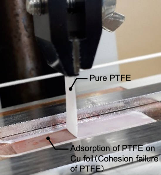
“Copper is the go-to wiring material for printed wiring boards because it is highly conductive, so the focus for improvement is to decrease transmission loss from the support material,” according to the university, “PTFE is ideal for this role because it has both low relative dielectric constant and low dielectric loss tangent, however PTFE does not like to stick to things.”

The Osaka technique requires no intermediate layer.
“Our technique involves heat-assisted plasma [HAP] treatment,” said resaercher Misa Nishino. “We subjected the PTFE to a HAP to make the surface stickier, and then pressed the two layers together at a high temperature to ensure they were strongly bonded.”
It was tested on both pure PTFE and a cloth woven from glass and PTFE, and worked with smooth surface copper foil.
“Our method is both simple and environmentally friendly, making it a highly attractive option for large scale processes,” says fellow resaercher Yuji Ohkubo. “We expect our findings will be used to make high-frequency printed wiring boards that will contribute to the enhancement of digital devices for the 5G world and beyond.”